Performance Features and Design of HT1200M
The HART (Highway Addressable Remote Transducer) protocol was launched by Rosemount Company in the United States in the mid-1980s. It is mainly used for digital communication between on-site intelligent instruments and control systems. The HART protocol superimposes audio digital signals on 4~20 mA analog signals. The digital signal amplitude is 0.5 mA and the data rate reaches 1200 b/s. 1200 Hz represents logic "1" and 2200 Hz represents logic "0". Enables two-way digital communication. HART communication has the characteristics of simultaneous point-to-point 4 ~ 20 mA analog and digital communication, multi-station communication methods, and multiple transmissions.
HT1200M features:
lSingle-chip, half-duplex 1200b/s frequency shift keying (FSK) modem
lBell202 standard FSK frequency shift keying signal, carrier wave is 1200Hz and 2200Hz
lInternally integrated receive bandpass filter circuit and transmit signal waveform shaping circuit
lExternal 460.8kHz crystal or ceramic filter internal clock oscillator or use external input clock
lOperating temperature: -40℃~+85℃
lPower supply voltage: 2.7V~5.0V
lMeet HART physical layer requirements
lSupport LQFP32 and QFN32 packaging
lFully compatible with HT20C15
lHT1200M pin definition and description
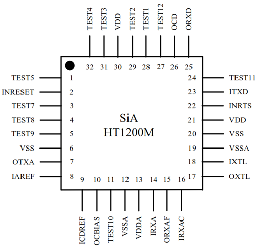
HT1200 chip LQFP32 & QFN32 pin distribution diagram
Pin | Definition | Type | Illustrate |
1 | TEST5 | Input | Connect to VSS |
2 | INRESET | Input | A low input resets all digital logic circuits |
3 | TEST7 | Input | Connect to VSS |
4 | TEST8 | Input | Connect to VSS |
5 | TEST9 | Input | Connect to VSS |
6 | VSS | Ground | Digital ground |
7 | OTXA | Output | The modulated FSK transmission signal is coupled to the 4-20mA circuit |
8 | IAREF | Input | Analog reference voltage |
9 | ICDREF | Input | Carrier sense reference voltage |
10 | OCBIAS | Output | Comparator bias current |
11 | TEST10 | Input | Connect to VSS |
12 | VSSA | Ground | Analog ground |
13 | VDDA | Power | Analog power input |
14 | IRXA | Input | FSK input signal received from 4-20mA circuit |
15 | ORXAF | Output | Analog receive filter output |
16 | IRXAC | Input | Analog receive comparator input |
17 | OXTL | Output | Crystal oscillator output |
18 | IXTL | Input | Crystal oscillator input |
19 | VSSA | Ground | Analog ground |
20 | VSS | Ground | Digital ground |
21 | VDD | Power | Digital power input |
22 | INRTS | Input | send request |
23 | ITXD | Input | Enter transfer data. HART data stream to be sent from UART |
24 | TEST11 | NC | Not connected |
25 | ORXD | Output | The received demodulated HART data is sent to the UART |
26 | OCD | Output | Carrier detect output |
27 | TEST12 | NC | Not connected |
28 | TEST1 | Input | Connect to VSS |
29 | TEST2 | NC | Not connected |
30 | VDD | Power | Digital power input |
31 | TEST3 | NC | Not connected |
32 | TEST4 | NC | Not connected |
Design of HART Protocol Communication Card Based on HT1200M
The HART protocol communication module is mainly composed of MCU, HT1200M and DA (the most commonly used currently is AD421) chips in the field instrument. The DA chip receives the digital signal transmitted by the MCU and converts it into a 4~20 mA current output, and the HT1200M receives the FSK signal superimposed on the 4~20mA loop. After demodulation, it is transmitted to MCU. Or the response information generated by the MCU is modulated into an FSK signal, passed through the waveform shaper, and then superimposed on the 4~20 mA loop by the DA chip and sent out. The following figure shows the structure block diagram of the HART communication module and the typical circuit schematic diagram of HT1200M.
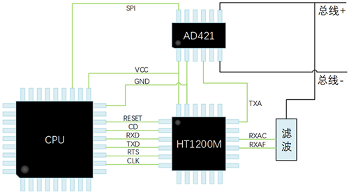
HART module structure block diagram
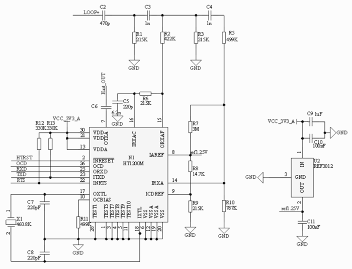
HT1200M typical circuit schematic diagram

